Evolution of deep learning is not just gated by algorithm development, but also evolution of hardware (one could make the argument that algorithm development itself is gated by hardware as well, but that’s a stronger point than I want to argue). For example, tracing the state of the art models for differnet tasks in the past few years:
- In 2015, Microsoft trained ResNet model with 60 million parameters, requiring 7 exaFLOPS
- In 2016, Baidu trained deep speech 2 with 300 million parameters, requiring 20 exaFLOPS
- In 2017, Google trained Neural Machine Translation with 7 billion parameters, requiring 100 exaFLOPS
This trend tells us that while many will work to reduce model size, preclude having to train and retrain models by better mechanisms for composition, and many other workstreams, we can expect to continue to see an increase in model size for improving state of the art benchmarks. Which begs the question: as our models grow in size (# of trainable parameters) and complexity, will the cost of training and inference rise linearly as well?
Moore’s Law, Amdahl’s Law and Dennard Scaling
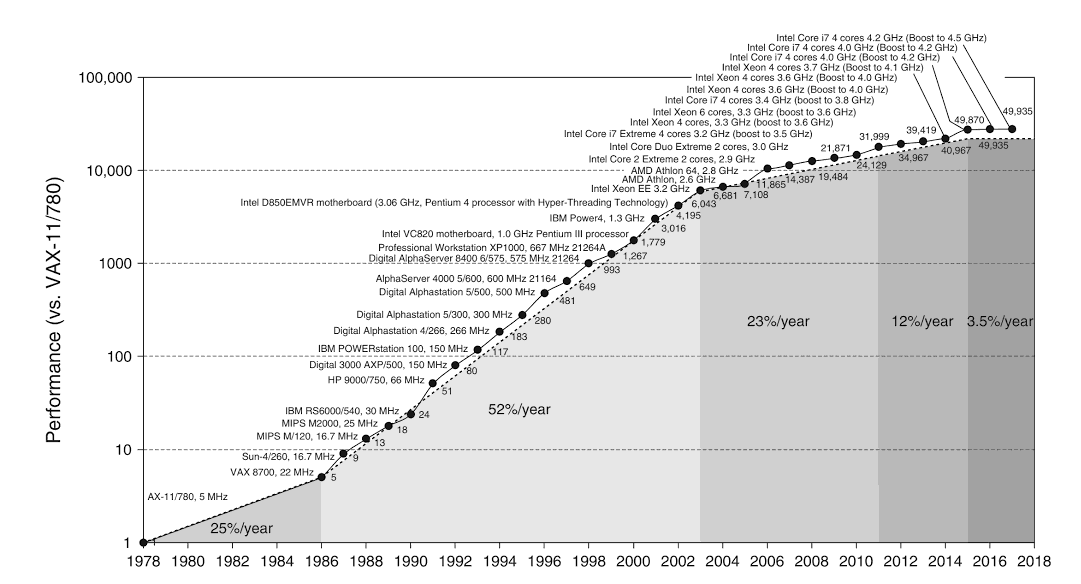
We have heard a lot about the death of Moore’s law. What does this mean for DL? Let’s recap: Moore’s law refers to the trend that # of components in integrated chips is doubling every 18 months. As we are all painfully aware, this pace started to slow around 2010. Let’s look at a picture taken from Hennessy and Patterson’s seminal textbook on computer architecture:

First, note that this means a high-end microprocessor today has about 50000 times the performance of a 1978 mini-computer (at less than 1% of the cost). Then notice that following the healthy 25% annual growth rate of the first decade or so, for almost 20 years, performance grew at about 50% a year, a doubling time of one and a half year.
The rate of growth started to stall at around 2004, due to the death of a related law: Dennard’s Scaling. In 1974, Dennard hypothesized that the power density is constant as transistors get smaller. This was based on the observation that as linear dimensions of a transistor shrank by a factor of 2 (the area shrinking by 4), we can reduce both the voltage and the current flowing through by 2, yielding the same power at the same frequency ( \(P = IV\) ). While the first half of the hypothesis remained true (we kept on reducing the size of transistors), the second half stopped being true around 2004, when we realized lowering the voltage and current below certain thresholds introduced reliability issues. This caused the rate of growth to drop to 23% until 2011, around the time when Moore’s Law also started to die out.
Gordon Moore himself in an interview in 2005 claimd “It can’t continue forever. The nature of exponentials is that you push them out and eventually disaster happens….in terms of size [of transistors] you can see that we’re approaching the size of atoms which is a fundamental barrier, but it’ll be two or three generations before we get that far—but that’s as far out as we’ve ever been able to see. We have another 10 to 20 years before we reach a fundamental limit. By then they’ll be able to make bigger chips and have transistor budgets in the billions.”
10 or 20 may have been a bit off; in 2016, after relying on Moore’s law for future forecasts since 1998, the International Technology Roadmap for Semiconductors shifted its focus to a plan outlined “More than Moore” strategy in which instead of incessant focus on semiconductor scaling, the needs of applications drive chip development.
As these two laws slowly fade out of the picture, so have computer architects’ efforts to turn increased resources into performance with sophisticated processor designs and memory hierarchies that without making the programmer think about it, exploited inherent instruction-level parallelism in seemingly serially designed code. Around 2005, architects started shifting their efforts from building a single processor per microprocessor to multiple efficient processors per chip.
As architects push the limits of the above (exploting instruction-level parallelism without requiring special thinking or work from the programmer), they start to bump up against limits imposed by Gene Amdahl’s law, which states that the theoretical speedup from parallelism is limited by the sequential part of the task. This means that how the programmer wrote down the instructions she wishes the machine to execute may make adding an \(n+1\) core to the processor pointless.
So where does this leave us? Let’s recap: Transistors are not getting any better (death of Moore’s Law), the power consumption per chip area is increasing (due to the fact that \(V\) and \(I\) levels can’t decrease at the same rate that transistors shrink, Dennard Scaling), the power budget per chip is not increasing (electro-migration and mechanical and thermal limits) and we have already exploited much of the multi-core card pattern that chip designers in the past counted on to increase performance (which is itself limited by Amdahl’s Law).
What does this mean for DL? Well it’s simple and we’re already doing it: specialization, at the hardware level. Specialized chips carrying out specialized instructions using specialized data pipelines in specialized data formats. This yields hardware that can only do a few tasks; but they do them extremely well (quickly and cheaply)!
TPUs v1
There is a famous story about Jeff Dean doing some back of the envelope calculations in 2013 and concluding that if Google users were to use the voice search functionality for ~3 minutes a day (which in turn were run on DL-based Automatic Speech Recognition models), and Google used all of its datacenters for serving these inference requests, they would need to double Google’s then-current resource footprint. Out of this existential threat was born the TPU project, setting out to build the a custom chip for inference (Google also started aggressively buying off-the-shelf GPUs for training around the same time as a stop-gap measure for training needs). We would later go on to build TPU v2 and v3 which allowed users to train and do inference on the same hardware platform, but the need for inference hardware was much more urgent and thus the first generation was an inference-only chip with a number of hard trade-offs made. As a rough timeline, the TPU v1 was designed, verified, built, and deployed in some of Google’s datacenters in just 15 months.
Requirements
A survey of Google DL production workloads in 2016 by Patterson et al [3] showed that ~95% of the neural architectures fit one of the following three categories:
- Multi-layered (~5 layers) perceptrons containing a range of 5-20M parameters [~60% of deployments]
- Long-Short Term Memory (~60 layers) containing a range of 30-50M parameters [~30% of deployments]
- Convolutional networks (20-100 layers) containing a range of 10-100s of Millions of parameters [~5% of deployments]
Furthermore, most doing inference on the DL models was found to usually be on the critical path of an applications response to an end-user request, so keeping 99th percentile (and sometime 99.9th percentile) tail latency down was of utmost importance. However, one quality of the models to be exploited was that unlike typical high-performance computing applications, most models could be tuned such that inference was done using quantized operations (discretizing floating point values to integers) without signficant accuracy hits, saving memory, compute and power. As a data point, size of the popular but large Inception model can be reduced from over 90MB to 23MB using just quantization. This allows the TPU to implement arithmetics using 8-bit integers rather than the expensive 32-bit floating-point multipliers used in most GPUs.
Technical Details
Due to the tight timeline, the team needed to make many tough decisions around hardware implementation complexity, to decrease chance of late-stage bug discovery. For example, much like GPUs, TPU v1 is actually a coprocessor on the I/O bus, rather than being tightly integrated with the CPU - this allows it to be able to be deployed by being plugged into existing servers’ SATA hard disk slot. However unlike a GPU, it does not fetch instructions from the host but rather relies on the CPU to feed it instructions (much like a Floating-Point Unit).
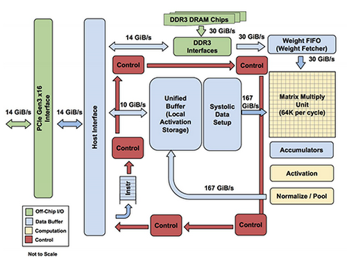
The TPU is built on a 28nm process running at 700MHz, consuming 40W when running. Below is a block diagram of the TPU v1:

As you may be able to guess from the block diagram, unlike CPUs designed in the 21st century, TPUs follow a CISC (Complex Instruction Set Computer) model. As mentioned before, the instructions are sent over a Peripheral Component Interconnect express (PCIe) at 14GB/s into an instruction buffer. At the heart of the TPU is a Matrix Multiply Unit (MXU) with 256x256 MACs (Multiply-Accumulate operation, implementing \(a \leftarrow a + (b*x)\)) performing eight-bit multiply-and-add operations on signed or unsigned integers. The resulting 16-bit products are collected in the 4MG Accumulators. The activations (non-linearities applied to weights after the multiply-add or the \(f()\) in \(C = f(Ax + b)\)) are kept in the activation unit.
CPUs (without vectorized instruction set extensions like AVX and SSE) are scalar processors, meaning they process a single data operation with each instruction. GPUs, and CPUs with vectorized instruction set extensions implement SIMD (Single Instruction Multiple Data) whereby each instruction will silmuntanously run over a one-dimensional vector of data. While that has a speedup over scalar processing, it does not implement multi-dimensional matrix multiplication as naturally.
At the heart of the TPU, the MXU is implemented using a systolic array, whereby instead of each ALU reading and writing a single value to registers between operations, it will read the value from the register once, and let it flow through the many side-by-side ALUs in the MXU, being operated on in each cycle. The TPU MXU has \(2^8 * 2^8 = 2^{16}\) ALUs, doing a multiply-add at \(7 * 10^8\) MHz, meaning it is doing about \(9.2 * 10^{13}\) operations or 9.2 TOPs.
This means, while with every clock cycle a CPU can do a few operations, (tens with vector extensions), and GPU can do thousands or tens of thousands, using its 64 thousand ALUs, a TPU can do hundreds of thousands of useful instructions, all without ever having to read or write to a register greatly reducing power consumption.
Another source of reduced power consumption is that, looking at the red blocks in the diagram, the control units take up less than the 2% of the total area of the chip; this is in part because of the simple control-logic design, which makes the chip much faster and more power efficient, but trading off the ability to do things like branch prediction, out-of-order execution, multiprocessing, speculative prefetching, address coalescing, context switching and many more extremely useful functionalities of modern CPUs that are not useful for DL applications.
Superior TCO
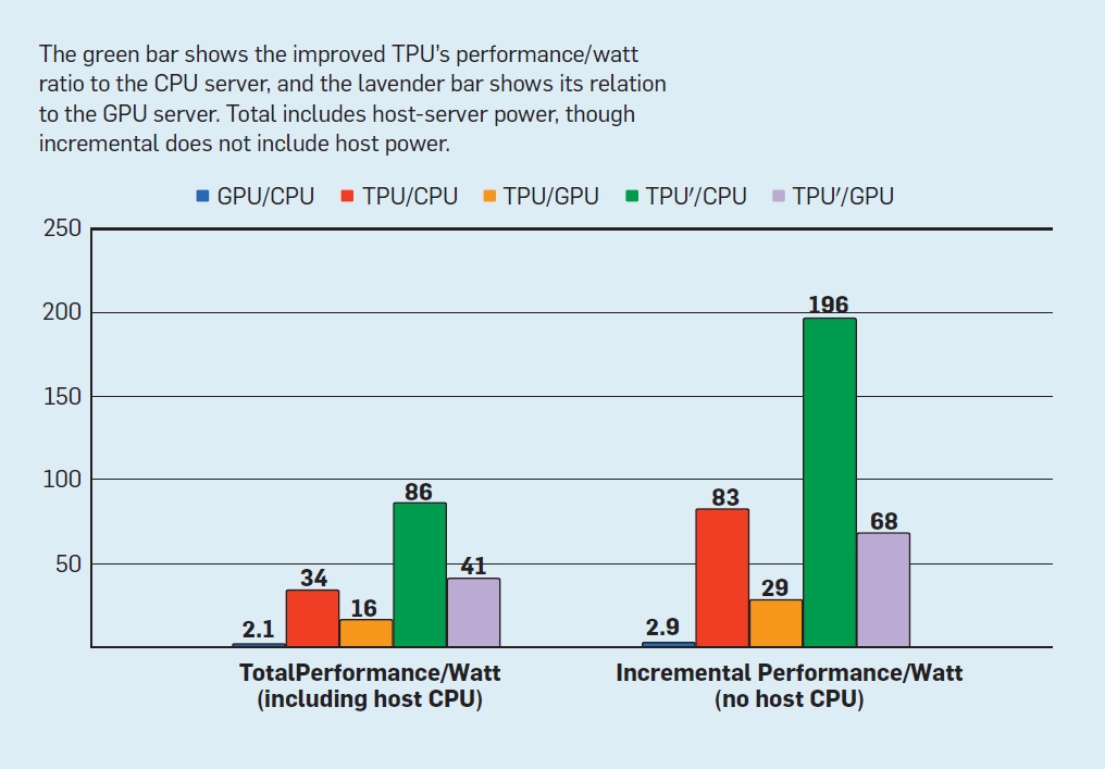
Perhaps the best cost metric for evaluating hardware in a datacenter is total cost of ownership (TCO), which while confidential for companies like Google, can be closely proxied via performance/Watt numbers.

There are many reasons for the improvements in the performance/cost ratio such as using 8-bit integers rather than 32-bit floating point ops, dropping unneeded CPU and GPU features, using a single large 2-d MXU instead of O(10) smaller, one-dimensional multiply units which do not suit matrix multiplication as well as 2-d hardware, and a single processor operating on single-threaded code, which not only improves power consumption, but also makes it easier for the system to stay within the tight tail latency budget requirements imposed by user-facing applications.
Note that TPU’ was a hypothetical TPU die that could be designed in the same process technology if the project was not under a hard deadline (by more aggressively working on logic synthesis and block design to improve the clock rate and using bettery memory circuitry to improve bandwidth.
Conclusion
The conclusion is that as with all engineering feats, the design of the TPU v1 was done by carefully making informed trade-offs to create a special-purpose accelerator. This was necessitated by the slowing down of compute hardware acceleration and the birth of DNNs and their unique requirements for hardware platforms. The design of TPUs was informed by requirements such as 10x lower TCO than GPU, low tail latency, support for dense linear algebra operations on hundreds of millions of parameters.
With these in mind, TPUs were designed and implemented to run DNNs up to 30 times faster with up to 80 times better energy efficiency than contemporary CPUs and GPUs, delivering 15-30 times better throughput while improving upon the tail latency observed using multi-threaded/chip CPUs and GPUs.
TODO: talk about support for sparsity, optimized data types and optimized data supply.
Sources
Computer Architecture by Hennessy and Patterson
Song Han’s lecture at Stanford